
| Home | S-100 Boards | History | New Boards | Software | Boards For Sale |
| Forum | Other Web Sites | Quiz | Index |
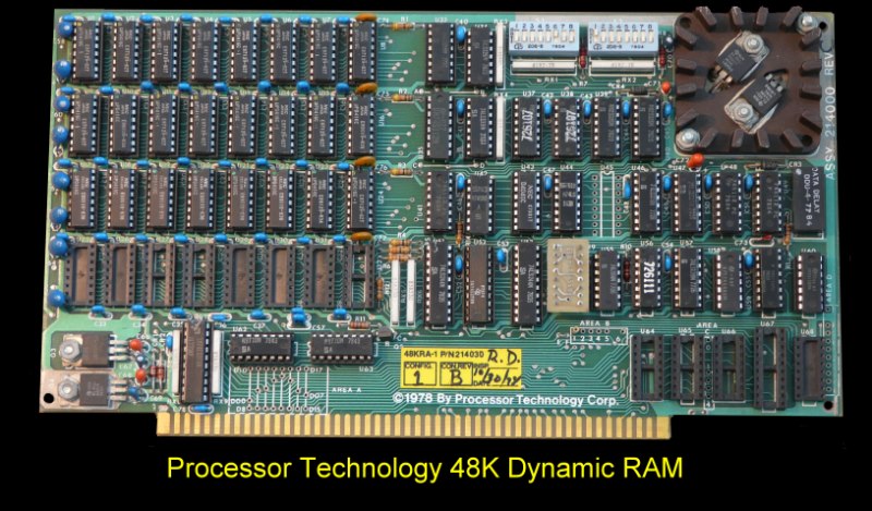
The three 16k pages (48k total) of populated memory chips on the board can be independently mapped over the normal 64k memory range of most S-100 computers using 16 address bits (section 3.2.2 of the manual) and only 8 data bits. The unpopulated 16k bank has to be left unmapped on the board as this is where you would have your EPROM mapped (on a different board) with the system monitor program, BIOS or boot loader program so that the addressing does not conflict with the addressing of the three 16k pages of dynamic RAM.
Sheet 1 of the schematic appears to be incomplete so I can't really decode all of the addressing options.
S-100 systems are capable of using up to 24 address bits which would allow for a total of 16 megabytes of memory to be mapped onto a system. This is where the empty bank of memory chips (U25-U32) and the empty sockets at U64 to U68 come in. U64-68 provide for extended address selection (see section 5.6 of the manual, unfortunately it appears to be incomplete) using the address lines A16-A23 so you can then populate the fourth row of dynamic RAM for a total of 64K of memory on the board. Then you could have a number of memory boards mapped at unique 64k intervals or 'banks' or 'pages' so they would not conflict with each other.
S-100 systems are also capable of up to 16 data bits -
that is what "Area A" on the board is for - so you could add jumpers to have
the data bus on the board mapped onto either the 8 upper or 8 lower data
bits. It may also be possible to set the board up to manipulate all 16 data
bits concurrently, but I can't tell without sheet 1 of the schematic.
Other Processor Technology S-100 Boards
This page was last modified on 07/31/2011